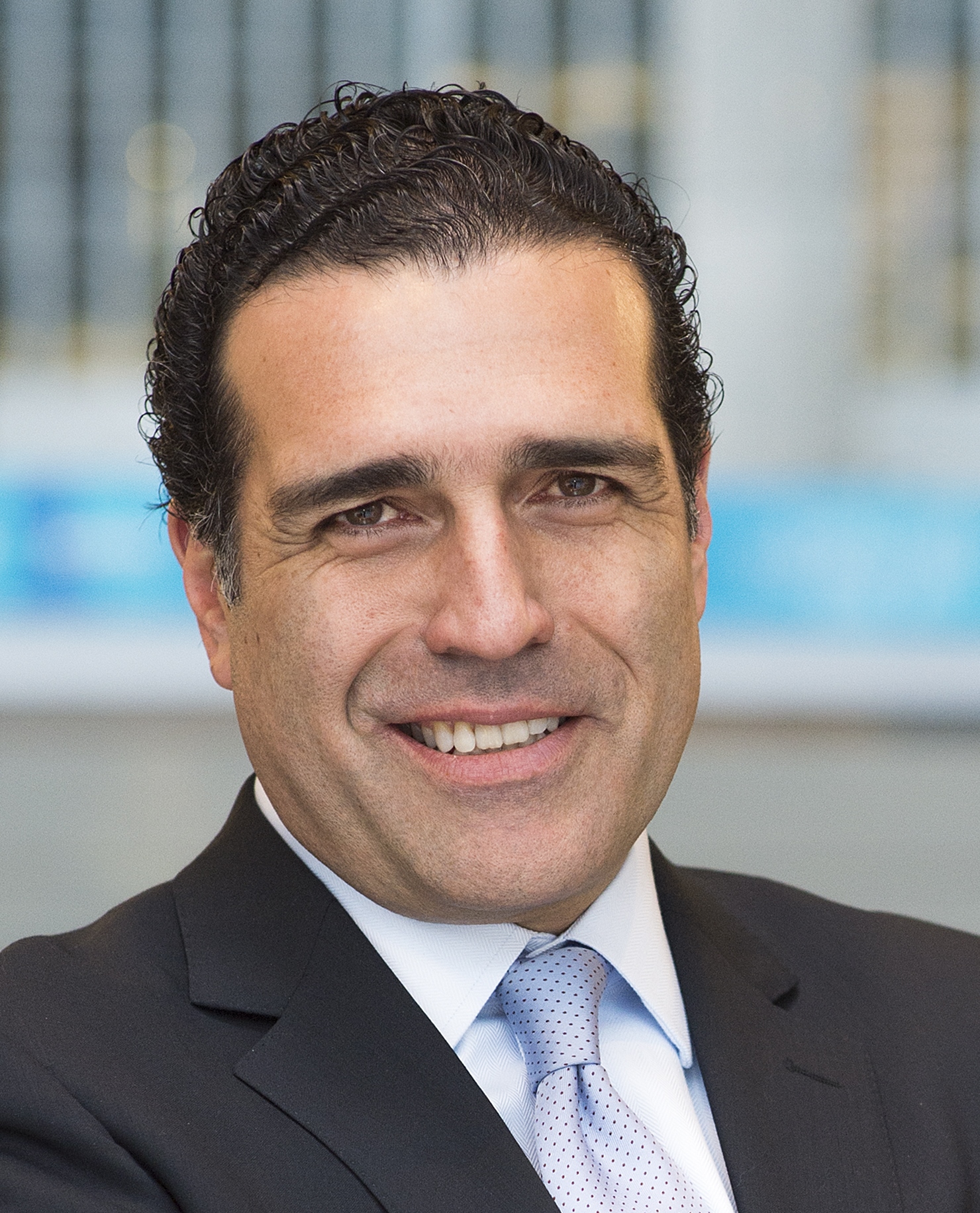
Dr. Haba joined Xperi (previously called Tessera) in 1996 and is now holding the position of Senior Technical Fellow and Vice President. Today, he is heading down the path finding team in the Electronic R&D Division. His latest activities include the development of 3D technologies for mobiles and servers alike. Dr. Haba worked at Google Data Center Platform Division as a senior staff officer. Before that, in 2002, he co-founded SiliconPipe Inc. a high-speed interconnects start-up company based in Silicon Valley that was acquired by Samsung. He also managed the advanced packaging R&D Division at Rambus. From 1988 to 1996, he worked for the NEC Central Research Laboratories in Tokyo, Japan, and for IBM Watson Research Center in New York, where he invested his time working on the applications of lasers in microelectronics.
Dr. Haba received his Ph.D. degree in materials science and engineering, in the field of solar energy in 1988 from Stanford University, California, . He also obtained two master’s degrees in applied physics and materials science from the same university. He received his BA degree in physics from the University of Bab-Ezzouar, Algeria, in 1980. Dr. Haba holds over 500 U.S. patents, and over 1400 patents and patent applications worldwide. He is listed among the top 100 most prolific inventors worldwide. In 2017, he opened the Haba Institute in Algeria to help young entrepreneurs. Dr. Haba has authored numerous technical publications. He has also participated in many conferences worldwide and was recognized on many occasions, including Wissam El Alem El-Djazairi in 2015, R&D 100 for most prestigious innovation in 2003, Frost Sullivan Award in 2013 and the opening of the Nasdaq in 2007.


